

“They said graphene would be in my phone by now”
A friend asked me this at a night market in Shenzhen, a paper cup of sugarcane juice in one hand and a three-year-old phone in the other. He had read the same headlines I had. Graphene is stronger than steel, thinner than paper, bends light and electricity in ways silicon cannot. It was going to change everything.
That was 2004, when two physicists in Manchester pulled a single layer of carbon atoms off a block of graphite using sticky tape. They won the Nobel Prize in 2010. A lot of people assumed the phones would follow shortly after.
They didn’t. Twenty years on, you can buy a graphene-heated jacket in a Chinese shopping mall, and there is graphene powder in some battery additives, coatings and tires. What you cannot buy is a phone with a graphene chip inside it. So what happened?
The honest answer is: nothing dramatic went wrong. A gap turned out to exist between making a piece of graphene and making useful graphene, and crossing it took far longer than the headlines implied. Two recent research directions show how that gap is being closed, and where it still holds.
What “wafer-scale” actually means
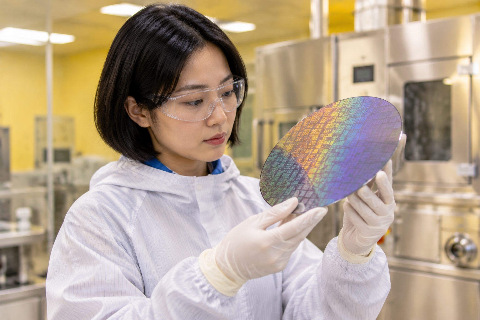
Start with a picture. The graphene that won a Nobel Prize was a flake the width of a human hair, made by hand, one at a time. It worked beautifully, as a physics experiment.
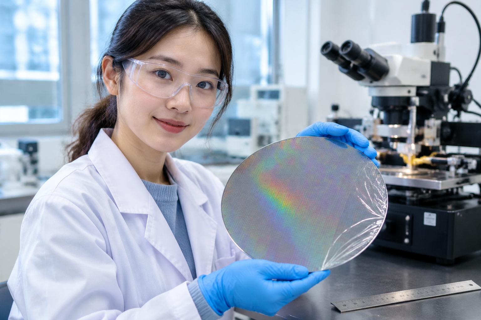
A chip factory needs something else entirely: a round disc of material called a wafer. Modern fabs run 200 mm or 300 mm wafers, about the size of a dinner plate. Research lines usually work smaller, at 100 mm or 150 mm. Every square millimetre of that disc has to behave the same way, because a single wafer gets carved into thousands of chips at once. If ten percent of the surface is defective, you have not made a cheap chip. You have made an expensive failure.
That is the difference between a lab result and a production capability. It is the difference between hand-stretching one perfect pizza dough and running a bakery that produces ten thousand identical pizzas a day, none of them torn.

Most large-area graphene is produced by chemical vapour deposition, or CVD: methane gas is passed over hot copper foil, and carbon atoms settle into a honeycomb layer on the metal. This part, growing the film, has been working at scale for years. Films on 4-inch, 6-inch and occasionally larger substrates have been reported by Chinese, Korean, American and European groups. The sizes vary from paper to paper, and the details matter.
The hard part comes next. The graphene has to be lifted off the copper and placed onto the wafer that will carry the device, without tearing it, wrinkling it, or leaving a polymer layer behind that ruins its electrical properties. Transfer is where promising films go to die, and much of the recent progress is really transfer engineering: roll-to-roll lamination, face-to-face bonding, and methods that skip the copper entirely.
Quantum rectification, in plain terms
Now for the second half of the story, which is a different kind of work and often gets muddled with the first.
A rectifier is a one-way valve for electricity. Your phone charger is full of them: they turn the alternating current from a wall socket into the direct current your battery needs. Ordinary diodes do this by joining two differently doped semiconductor regions, and they pay a price. Some voltage is lost, some energy becomes heat, and at very high frequencies they simply cannot switch fast enough.
Quantum rectification does the same job using the quantum behaviour of electrons rather than a doped junction. Instead of a chemical interface, you build a tiny asymmetry: a thin insulating barrier, or a landscape where electrons moving one way face an easy path and electrons moving the other way face a wall. Because the effect comes from how electrons tunnel and how their energy states line up, it can happen at very low voltages and potentially at extremely high frequencies.
Graphene is interesting here because its electrons behave as if they have no mass. They travel ballistically over respectable distances and respond to electric fields in unusually shaped ways, which makes it easier to design an asymmetric structure at the atomic scale. The practical targets are low-power circuits and, further out, rectennas: tiny antennas that would capture ambient radio waves and convert them to a trickle of usable electricity.
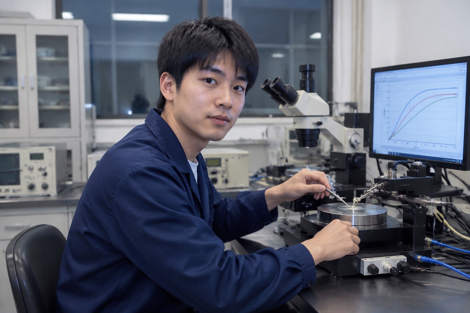
Keep this in proportion. Most quantum rectification results are single devices or small arrays, measured on a probe station, sometimes at room temperature, sometimes cooled to a few kelvin. They are genuine physics. They are not yet manufacturing.
The chain is longer than the breakthrough
People who work on this rarely talk about a single moment of success. They talk about a chain, and the weakest link moves.
Growth uniformity comes first: same thickness, same grain structure, same properties across the wafer, not just at the centre.
Transfer comes second, as above. Any residue from the supporting polymer shows up later as contact resistance.
Contacts and doping come third. Getting a metal to touch graphene with low resistance and keep it that way for years, through heat and humidity, is a materials problem that outlasts most research grants.
Fab compatibility comes fourth, and it is the quiet killer. A silicon fab operates under contamination rules that treat stray carbon as a threat. Getting a graphene step into an existing production line means convincing process engineers to change their floor, not just their papers.
Reliability testing comes last and takes the longest. Nobody buys a chip that has only been measured for six months.
How to read the next graphene headline
When a press release lands in your feed, five questions will tell you more than the headline:
1. What size? A square millimetre and a 150 mm wafer are different achievements dressed in the same words.
2. How many devices? One transistor is a demonstration. Ten thousand identical transistors with a yield figure is engineering.
3. Measured where? On-chip, on-wafer, in a package? Packaging can destroy a good result.
4. Under what conditions? If it only works at four kelvin, it is real science and a distant product.
5. Reproduced by whom? Independent repetition is the number that matters most, and the one least likely to appear in the announcement.
What ordinary people should take from it
China has become one of the largest centres of graphene research and processing. Industrial clusters in Jiangsu, around Changzhou and Wuxi, host companies making graphene powders, films and composite materials. Universities and national labs publish steadily alongside Korean, European and American teams. This is not a race with one winner; it is a long, distributed grind.
The visible products so far are unglamorous. Graphene heating films in electric vehicle battery packs, conductive additives in batteries, anti-corrosion coatings, composite plastics. None of them sound like the future. All of them are what a new material actually looks like when it starts paying its rent.
So when my friend at the night market asked whether graphene was a scam, I said no, but also that it was not the right question. The right question is what has to be true before it makes sense to put it in a phone. A wafer that a fab can handle. A transfer process that doesn’t ruin it. Contacts that survive a decade. A product where its advantages outweigh the cost of switching the entire supply chain.
That work is happening, slowly, in labs with yellow lighting and probe stations. It does not produce good headlines. It produces wafers.